Lab 1 Report
Introduction
In this lab, we built out motherboard with the FPGA and the microcontroller through soldering, and tested our board by loading designs onto our FPGA nad microcontroller. We implemented a design on the FPGA to test the on-board high-speed oscillator by blinking one of the on-board LEDs. And we implemented a program on the microcontroller to light an LED.
Overall, the main goal after creating our boards was to create a seven segment display. We wrote verilog to convert a 4-bit hex inputted through a switch into display using 7-segments. We did this by programming pins on the FPGA based on the switches, and then connecting this to a physical build of a seven-segment display on a breadboard to observe the numbers. We also used the switches to light other LEDs on the FPGA, and like described earlier, we used the on-board high-speed oscillator to blind an on-board led at 2.4Hz.
Design and Testing Methodology
There were two different steps associated with the hardware component of the design, with the first one being the soldering of the components.
There were two main parts to soldering the components to the motherboard - we had to solder on the SMD components, and the THT components as well. We also soldered on the FPGA and micro-controller as well.
After the soldering was done, we proceeded to test our board. We first loaded a test program to the FPGA which uses the high-speed oscillator (HSOSC) from the iCE40 UltraPlus primitve library. Here, this library is used to generate a clock signal at 24Mhz, and then counter was implemented in order to produce a blinking frequency of 1.5Hz, so that we could see it on the LEDs. This was developed with a clock-divider module. After this, we uploaded another program to our FPGA which toggles pin P25 at around 1Hz, and if switch SW7 is on, then P25 is connected to PA9 which will see LED D3 blinking. We then, uploaded a program to our MCU unit, which reads the value of the toggled LED from the FPGA and echoes it to another pin which then causes LED D2 blinking.
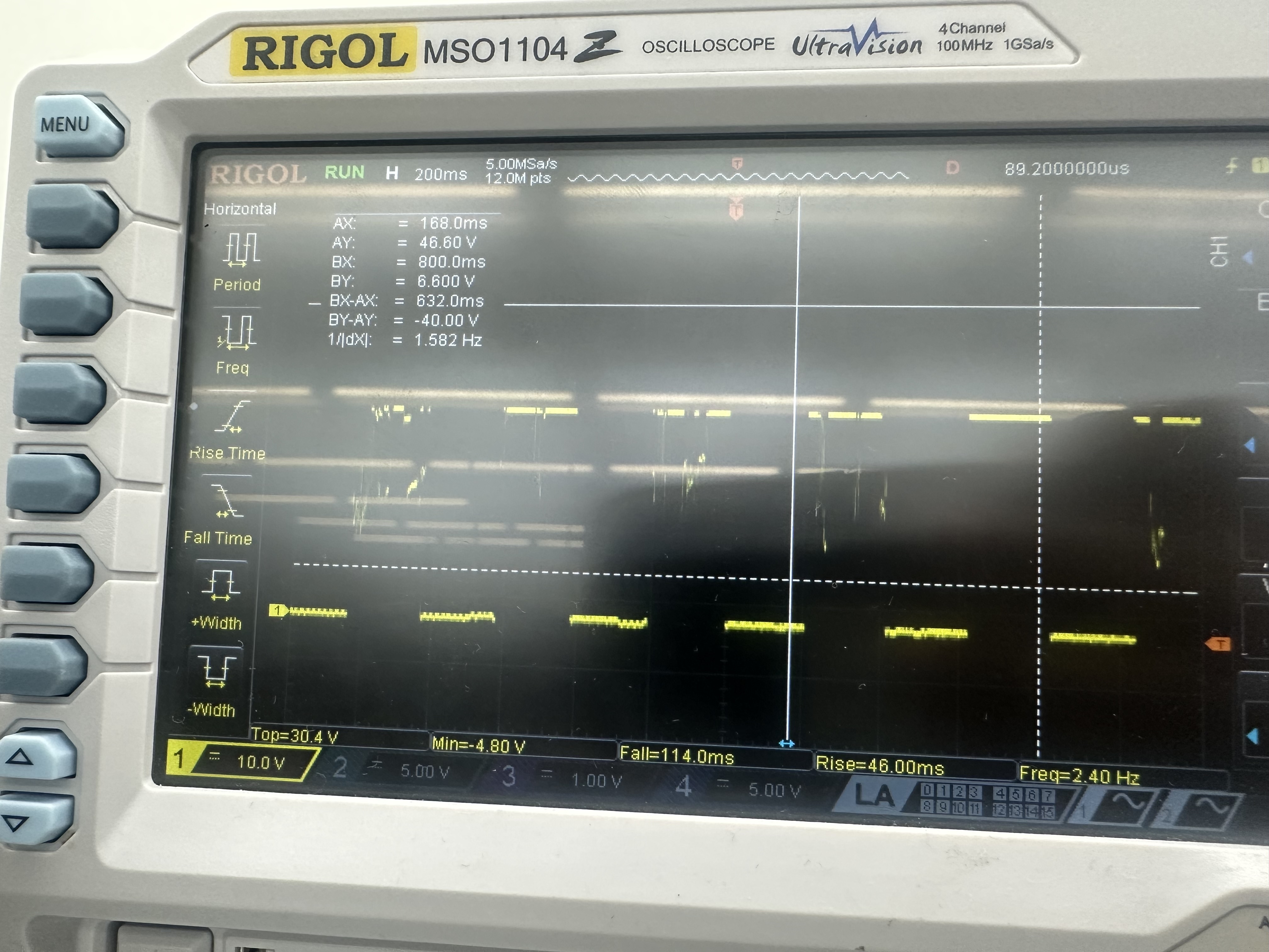
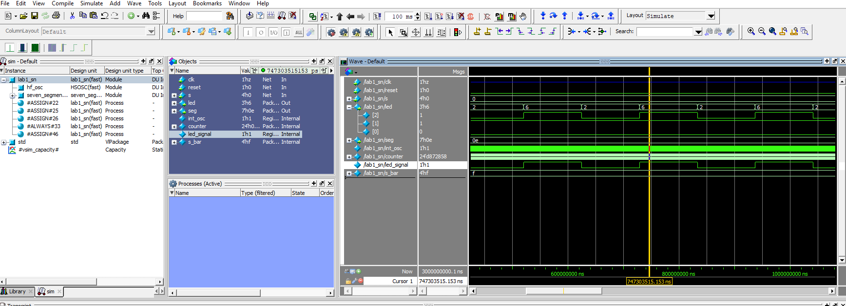
We then implemented the 7-segment code in verilog, which was essetially a decoder. Along with this, we programmed some switch inputs to control 3 other on-board FPGA LEDs using combinational logic, and using the HSOSC to take teh 24MHz signal and convert it into a 2.4Hz signal which was reflected in a blinking LED. I then used an oscilliscope to test the frequency of the blinking LED and it was exactly 2.4Hz. Figure 1 below shows this.
After this, we had to build the 7-segment LED display on a breadboard. After looking at the specs, I was able to apply power to one of the middle pins on either side, and ground the respective other pins in order to turn on that respective segment. Each non-power pin on the displaywas then hooked to ground through a 10kohm resistor. I made sure to connect the programmed pins from the FPGA to the seven-segment display. In order to test this, I created a self-checking testbench which ran through all posisble inputs and made sure the outputs were as expected.
Technical Documentation:
The source code for the project can be found in the associated Github repository
Block Diagram
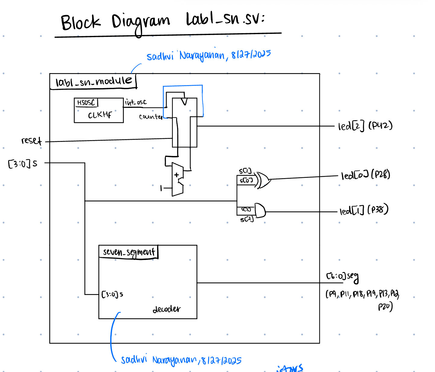 The block diagram in Figure 2 demonstrates the overall design and architecture of the design. The top-level module incldes two sub-modules - the HSOSC (high-speed oscillator block), and the seven_segment module in order to convert hex digits to seven segments. Additionally, there is internal counter logic fro the clock divider, as well as combinational logic to control the LEDs.
Schematic
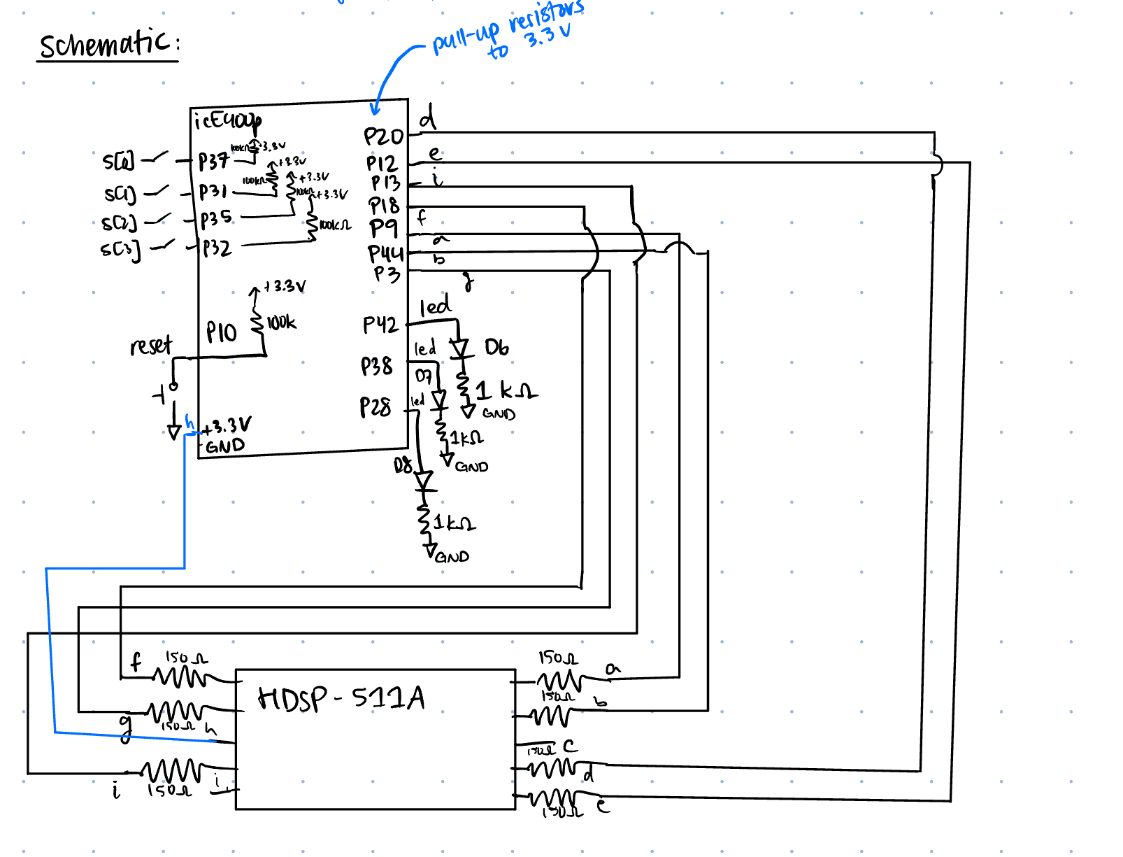 Figure 3 demonstrates the physical layout of the design. We have internal 100k-ohm pullup resistors in order to ensure the pins aren’t floating. We then have the output on-board LEDs connected using a 1k-ohm current limiting resistor to ensure the output current (around 2.6mA) did not exceed the maximum output current of the FPGA I/O pins.
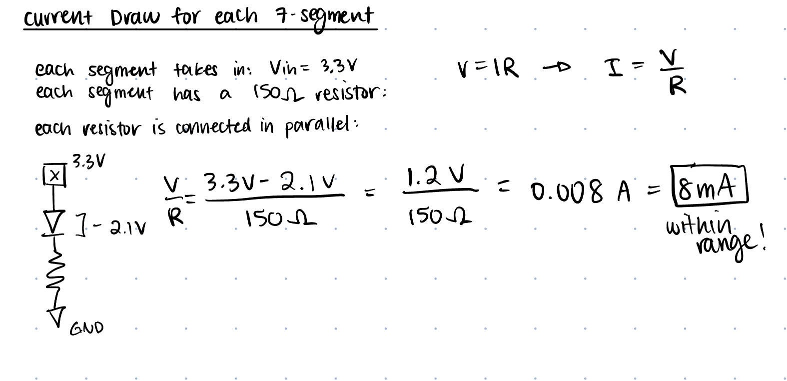
Then, if we look further down, we can see the seven-segment display component. Here we power the middle pin on the left, which propogates to all the other pins. In order to turn on a pin, it needs to be grounded, hence we have 10k-ohm resistors connected from each output pin to ground in order to not exceed the maximum allowed output current of the pins. Figure 4 highlights the calculations performed to ensure we were not exceeding the maximum current allowed.
Results and Discussion
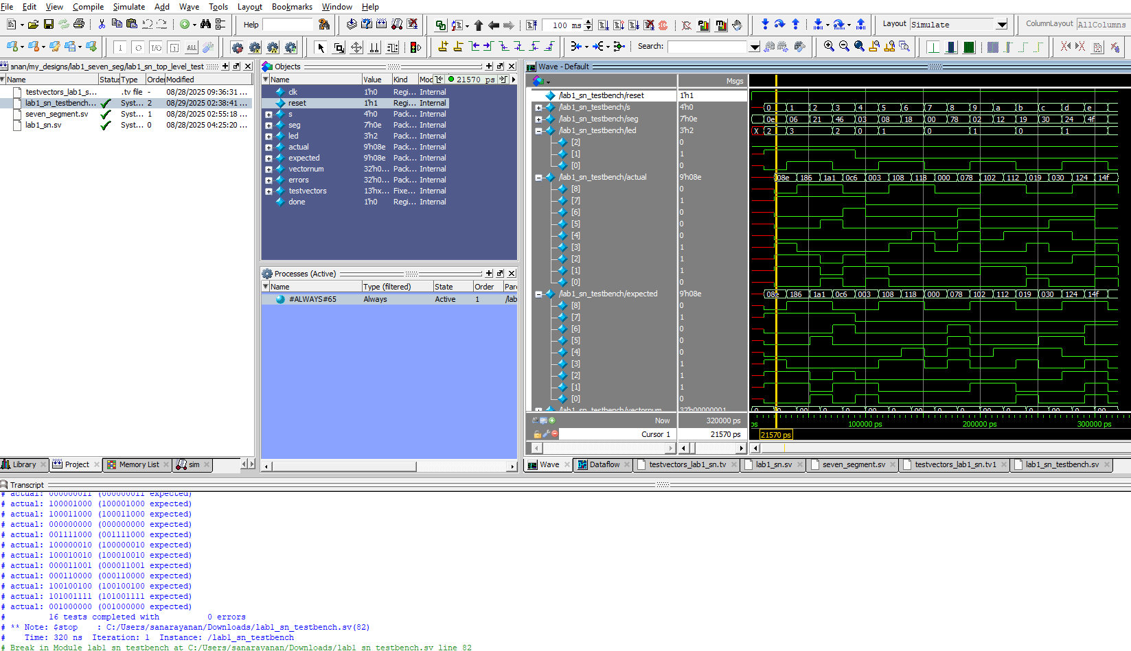
I was able to accomplish all of the prescribed tasks in this project. I also met all the intended design objectives, and was able to check off all the components in the spec, along with the excellence components. Figure 5 shows a screenshot of the QuestaSim Simulation. This is the simulation run with the self checking test-bench.
Figure 6 on the other hand, shows the toggling of led 2 at 2.4Hz using the clock divider. If I was given more time, I would have expanded the testbench to also test that the led signal was infact blinking at 2.4Hz through possibly another clock generation. The design performed exactly as intended, with the blinking LEDs blinking at the approproate frequencies, and the seven segment display working exactly as intended.
Conclusion
The overall design, after all the testing, successfully takes a 4-bit hex number inputted by the user on the DIP switches, and then converts this into the numeric hex representation of this number on the seven-segment display. I spent a total of 25 hours working on this lab.
AI Prototype Summary
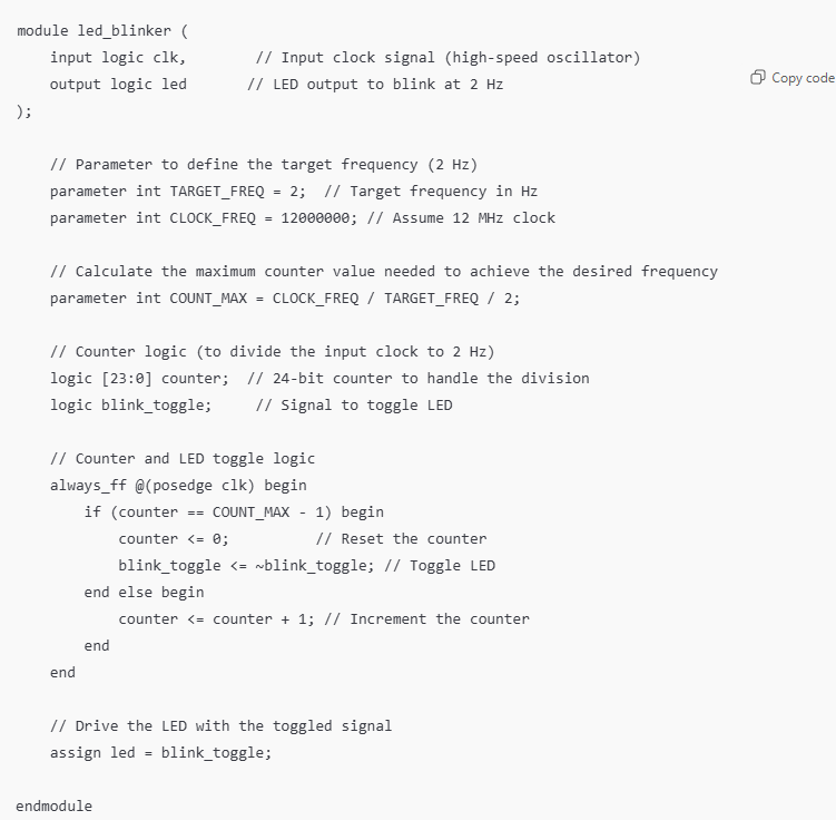
Figure 7 shows the result of entering the prompt into ChatGPT.
After entering this project into Lattice, and synthesiszing it, it seemed to have run with no errors, meaning at least the verilog syntax was correct. Additionally, it seems like most of the logic is correct for the counter, and it even accounted for dividing the period by 2 in order to toggle two times in each period. Figure 8 shows the successful response.
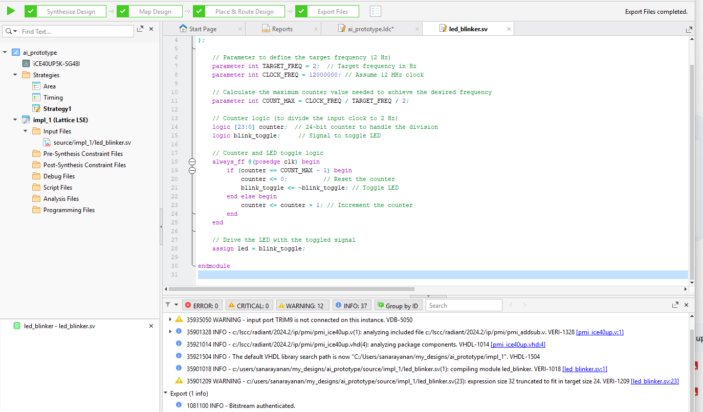
Overall, I would say that the quality of this verilog is really nice, with a very exact counter. This was similar to how I learned it in E85 last semester for my music lab, and therefore how I implemented it myself. The LLM did generate some constructs like parameter int, which I have never used before. The code did synthesize the first time around, which is impressive. However, this is also a common application of clock dividing, so it must have been trained on a lot of relevant data. There were very small errors such as bit truncation for optimization.
Next time I use LLM in my workflow, it is important to understand how to prompt the model, it is important to give it the constraints you are working under, and even providing specific library names are important. I was really surprised when the LLM picked up on the HSOSC library and the documentation for the syntax.