E155 Project Proposal: FPGA + MCU Slot Machine
Project Description and Overview
The goal is to create a functional, visually engaging slot machine simulation that:
Accepts a penny slot and “spin” button input.
Displays animated reels on a VGA output.
Sequentially stops each reel to show a final symbol combination determined randomly by the MCU.
Calculates and displays winnings and total credits based on the result.
The FPGA will handle video display including sending information to the VGA and time-sensitive animations, while the MCU will manage the actual game logic/state, input handling, and random number generation.
The system will include: - Three spinning reels rendered on a VGA monitor.
A coin slot, push buttons, and a switch for user interaction:
Spin Button — initiates reel animation.
Denomination Switch - indicated how much to bet per spin
Coin Slot — triggers an interrupt and increments credits using an LED to photo diode monitor
5 seven segment displays, 2 for credits won on the previous spin, and 3 for total credits accrued
The design will interface the MCU and FPGA via SPI communication, allowing the FPGA to render and display the visual state based on the game logic computed by the MCU.
Block Diagram
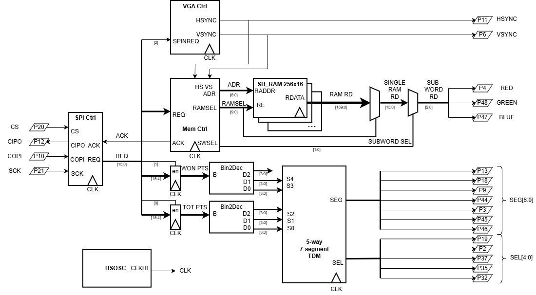
The block diagram in Figure 1 demonstrates the overall design and architecture of the design. We can see there are a variety of control modules to handle the VGA display as well as memory accesses (to display the sprites correctly). We also have ROM blocks, and other elements include a SPI module and 7-segment display for other feautures in our design.
FPGA Design
The FPGA handles visual, and time-sensitive operations such as VGA output and reel animation.
Core FPGA Modules
- VGA Controller
- Generates horizontal and vertical sync signals (
hcount,vcount) - Drives RGB output based on current reel state
- Continuously renders symbols based on current positions
- Generates horizontal and vertical sync signals (
- Memory Controller
- Gets reel ending symbol index from MCU and adds a 1-pixel offset based on counters
- Takes in
(x, y)coordinates from VGA controller to calculate what reel it’s on and translate this to RGB color
- Handles:
- Big pixel line and number of times to display that line (fixed number = X, determines pixel size)
- Once a big pixel line is displayed X times and repeated N = 10 times → one sprite is done
- Then increments sprite counter and restarts process
- Sequentially stops reels in timed order (each following reel performs one full rotation before stopping for a randomized look)
- For each reel, store a count N (reel 1 → 5, reel 2 → 6, reel 3 → 7)
- Once the ending symbol index of each reel has fully rendered N times, stop spinning that reel
- Reels stop at the precomputed random position sent over by the MCU
- Once all reels stop, accept
WINmessage from MCU and update winnings
- FPGA knows when it’s stopped spinning, so it continues to send the same pixels to VGA to hold state
- Symbol ROM Storage
- Stores a contiguous block of equal-sized frames for symbols
- Defines memory layout for each reel (symbol order used to index into memory)
- FPGA cycles through these addresses for the three reels
- SPI Interface Module
- Receives 16-bit commands from MCU and returns an acknowledge signal (
ACK) in the LSB
- 12 bits of data, 4 bits for request encoding (
REQ) REQ == SPIN→ 12 bits contain final 4-bit indices of the 3 reels
REQ == WIN→ 12 bits contain the number of points won on that spin
REQ == UPDATE→ 12 bits contain the total number of points
- (Optional): Display a win/lose message on the VGA display
- Receives 16-bit commands from MCU and returns an acknowledge signal (
- LED Display Controller
- Displays credits won and total credits on seven-segment displays
MCU Design
The MCU handles high-level game logic and asynchronous events.
Core MCU Functions:
- Coin Detection (Interrupt-Driven):
- External interrupt triggered by photodiode/coin slot.
- Increments credit count
- Denomination dial determines number of credits to “bet”
- Only starts game when denomination is less that or equal to number of credits
- Button Handling:
- Spin button Interrupt triggers START_SPIN sequence and message to FPGA
- Game Logic:
- Tracks credits, bets, and game state (
IDLE,SPINNING,RESULT). - Generates the true random final indices of the displayed icons from within three lists representing the three spinning reels, using these to calculate the player’s winnings and total credits
- Sends a 16 bit SPI packet to the FPGA to indicate where the three reels should stop spinning, then another for how many credits the player won, and a final one for how many credits the player has
- Waits for an ACK between all three
- Tracks credits, bets, and game state (
- Audio Control (optional):
- PWM-based simple tone for win/lose feedback.
Task Breakdown
| Task | Estimated Turnaround | Owner |
|---|---|---|
| Project Proposal (this document) | 1 week | Shared |
| VGA Output from FPGA | 3 weeks | Sadhvi |
| Symbol Digital Art | 1 week | Shared |
| Seven Segment Display Output | 1 week | Shared (essentially done) |
| FPGA SPI interface (peripheral) | 1 week | Sadhvi |
| Block level formal verification | 1 week | Corey |
| Full RTL functional verification | 1 week | Corey |
| Design Review Presentation | 1 week | Shared |
| MCU button/coin slot interrupts | 1 week | Corey |
| MCU SPI output (controller) | 1 week | Corey |
| MCU Main Game Logic | 1 week | Corey |
| Physical Assembly | 1 week | Corey |
| Final Report | 1 week | Shared |
Project Schedule
| Project Week | End Date | Expected Deliverables |
|---|---|---|
| 1 | Thurs Oct 16 | Project Proposal (this document) |
| 2 | Thurs Oct 23 | Orders placed for long turnaround parts |
| 3 | Thurs Oct 30 | RTL block specifications, Game icon artwork |
| 4 | Thurs Nov 6 | Design Review Presentation, VGA driver testbench/SVA, seven segment driver testbench/SVA, Seven segment driver RTL, SPI interface testbench/SVA |
| 5 | Thurs Nov 13 | System level testbench, VGA output on FPGA (hard coded example spin), SPI interface RTL, Button and coin slot interrupts on MCU, All circuits breadboarded |
| 6 | Thurs Nov 20 | Midpoint demo report, SPI output on MCU (dummy transactions for hardware FPGA testing), VGA output from SPI transaction, Seven segment output from SPI transactions, Game logic C code |
| 7 | Tues Nov 25 | Physical Assembly, Whole system hardware validation |
| 8 | Thurs Dec 4 | Projects Demo Day, Final report |
Specifications
Bill of Materials
| Quantity | Item | Price (incl. Tax & Shipping) | Purchase Link |
|---|---|---|---|
| 1 | 7 inch VGA Monitor | $45.68 | Link to Monitor |
| 1 | Phototransistor | Stockroom | n/a |
| 1 | IR LED | Stockroom | n/a |
| 1 | Clicky Pushbutton | Stockroom | n/a |
| 1 | 4 Way (Rotary) Selector Switch | Stockroom | n/a |
| 5 | Seven Segment Display | Stockroom | n/a |
| 5 | PNP Transistors | Stockroom | n/a |
| 5 | 1 kΩ Resistors (for PNPs) | Stockroom | n/a |
| 7 | 680 Ω Resistors (current limiting) | Stockroom | n/a |
| 1 | 8 Ω Speaker | Stockroom | n/a |
| 1 | LM386 Audio Amplifier | Stockroom | n/a |
| 1 | 250 µF Capacitor | Stockroom | n/a |
| 1 | 10 µF Capacitor | Stockroom | n/a |
| 3 | 0.05 µF Capacitors | Stockroom | n/a |
Riskiest part of the design
VGA timing precision + display: Sending the correct pixels, at the correct rate, in the expected format, with the expected timing to the VGA from the FPGA
Design Specific Calculations
Predicted Number of LUTs in the design
- ( 20 flops (internal counters) + 24 flops (credit display) + 5 flops (seven-segment control output) + 64 flops (internal counter flops) + 16 flops (SPI) ) * 3 = 387 LUTs
Pixel Update Clock
- Pixel clock = horizontal total * vertical total * frame rate = 640 * 480 * 20Hz (slower frame rate to allow for memory accesses) = 6,144,000 Hz = 6.1 MHz