Documentation
New Hardware used by our Project
- FPGA: Embedded Block RAM (EBR)
The iCE40 FPGA includes dedicated memory blocks called EBRs, which we used to store all the sprite data for the slot machine symbols. These are separate from the regular LUT logic, so using them frees up LUTs for other parts of the design like our memory controller, VGA controller, SPI transactions etc., especially because we did have a lot of pipelined and combinational logic. Each symbol we used gets stored as a chunk of pixel data in EBR, where we store a 64x64 pixel resolution, and eventually scale it to 128x128 in the VGA. We need 4 ROM blocks per sprite, and on each word we store 4 pixels (each taking up 4 bits, where although we only need 3 using 4 can make logic easier because it allows us to use bit shifting instead of the division operator). The block configuration we used for the EBRs was 256x16. The memory controller reads from these blocks based on the current VGA position and which reel is being displayed. Our EBRs had a two cycle latency because it was using registered outputs as well. Essentially, our symbols are stored sequentially in memory, and the controller calculates the right address offset based on the reel position. When a reel is spinning, the offset keeps changing upon each frame to create the scrolling effect.
- MCU: True Random Number Generator (TRNG)
The STM32L4 has a “true” hardware random number generator that we used to pick where the reels end up. This approach allows us to use analog signals from physical noise in the chip’s circuits to create a true random seed instead of having a software defined pseudo-random number generator. When the player hits the spin button, the MCU gets random values from the TRNG peripheral and uses them to calculate the stopping positions for all three reels. Then the ending sprites for each reel gets sent to the FPGA over SPI, and the visual animation of the spinning reel begins. Using this form of hardware randomness makes the game more fair as you cannot take advantage of a known seed when generating the randomness.
Schematic
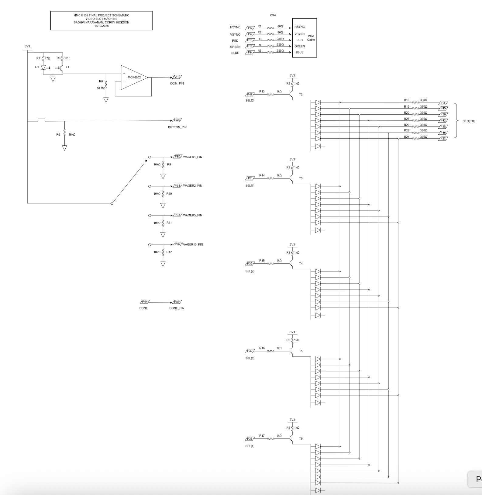
The schematic in Figure 1 demonstrates the overall design of how we are connecting the FPGA to the VGA monitor. Because we are only using 3-bit resolution for the pixels, we are scaling the voltage outputs to 0.7 if we want to display a color.
NOTE: Any pins with a letter following the “P” corresponds to a pin on the MCU (e.g. PA10, PB4), and any pin with just a number following “P” corresponds to a pin on the FPGA (e.g. P21, P47).
Technical Documentation/Source Code
The source code for the project can be found in the associated Github repository
Bill of Materials
| Quantity | Item | Price (incl. Tax & Shipping) | Purchase Link |
|---|---|---|---|
| 1 | 7 inch VGA Monitor | $45.68 | Link to Monitor |
| 1 | VGA Cable | Stockroom | n/a |
| 1 | Phototransistor | Stockroom | n/a |
| 1 | LED | Stockroom | n/a |
| 1 | Clicky Pushbutton | Stockroom | n/a |
| 1 | 4 Way (Rotary) Selector Switch | Stockroom | n/a |
| 5 | Seven Segment Display | Stockroom | n/a |
| 5 | PNP Transistors | Stockroom | n/a |
| 11 | 1 kΩ Resistors | Stockroom | n/a |
| 7 | 330 Ω Resistors | Stockroom | n/a |
| 5 | 10 kΩ Resistors | Stockroom | n/a |
| 1 | 10 MΩ Resistor | Stockroom | n/a |
| 1 | 47 Ω Resistor | Stockroom | n/a |
| 2 | 80 Ω Resistor | Stockroom | n/a |
| 3 | 280 Ω Resistor | Stockroom | n/a |
| 1 | MCP6002 Op Amp | Stockroom | n/a |